


NCKU Interdisciplinary Research Published in Nature: Atomic Stacking Restores Light Emission in Bilayer 2D Semiconductors
Written & Image credit to Kuang-I Lin.
Taiwan's semiconductor research has achieved another significant milestone. As transistor miniaturization approaches its physical and manufacturing limits, the global semiconductor industry is entering the post-Moore era, in which the development of novel semiconductor materials has become a major focus of international research. Dr. Kuang-I Lin of the Core Facility Center at National Cheng Kung University (NCKU), who also serves as an adjunct assistant professor at the Academy of Innovative Semiconductor and Sustainable Manufacturing, collaborated with an interdisciplinary research team from multiple institutions to achieve precise control over the atomic stacking configuration of bilayer molybdenum disulfide (MoS₂) using chemical vapor deposition (CVD). The team successfully synthesized a unique 1H-stacked MoS₂ bilayer that overcomes the indirect-bandgap limitations of conventional bilayer MoS₂, enabling a direct bandgap and remarkable valley polarization properties. This breakthrough was published in the October 1, 2026 issue of the prestigious international scientific journal Nature. Publication: Nature, Volume 658, pp. 71–77 (2026) Article title: Stacking-induced direct band gap in CVD-grown 1H MoS₂ bilayers

The research team successfully employed chemical vapor deposition (CVD) to precisely control the atomic stacking configuration of bilayer molybdenum disulfide (MoS₂), producing a unique 1H-stacked structure that exhibits a direct bandgap and remarkable valley polarization properties. The illustration depicts the atomic structure and optical characteristics of 1H-stacked bilayer MoS₂.
NCKU noted that silicon remains the dominant material used in semiconductor transistors. For decades, the semiconductor industry has followed Moore's Law, continuously reducing transistor dimensions and increasing transistor density on integrated circuits to improve computing performance and advance technology. However, as devices continue to shrink, physical constraints, manufacturing complexity, and production costs have become increasingly challenging. Consequently, semiconductor development can no longer rely solely on device miniaturization. Instead, the industry is actively exploring new materials, device architectures, and heterogeneous integration technologies to identify new opportunities in the post-Moore era.
The 2010 Nobel Prize in Physics recognized groundbreaking research on graphene, opening new possibilities in semiconductor and materials science. Both graphene and MoS₂ belong to the family of two-dimensional (2D) materials, characterized by atomic-scale thickness and distinctive electronic and optical properties. These materials are widely regarded as promising candidates for next-generation semiconductor devices. In particular, MoS₂ has attracted considerable international research interest because of its semiconducting properties and potential applications in optoelectronics.

Dr. Kuang-I Lin of National Cheng Kung University, in collaboration with Professor Yann-Wen Lan of National Taiwan Normal University and an interdisciplinary research team from multiple institutions, achieved a significant scientific breakthrough. The findings were published in the October 1 issue of the prestigious international scientific journal Nature.
The study was jointly led by four corresponding authors: Dr. Kuang-I Lin, Assistant Research Fellow and Chief Technology Officer for Nondestructive Analysis at NCKU's Core Facility Center; Professor Yann-Wen Lan, Professor Ting-Hua Lu, and postdoctoral researcher Dr. Tilo H. Yang of the Department of Physics at National Taiwan Normal University. The collaboration also involved research teams from National Taiwan University, National Yang Ming Chiao Tung University, and the National Synchrotron Radiation Research Center. By integrating expertise in material growth, advanced characterization, theoretical calculations, and spectroscopic measurements, the team demonstrated the strength of interdisciplinary and interinstitutional scientific collaboration.
Dr. Lin explained that the groundbreaking discovery of graphene originated from an unconventional approach to material preparation. By repeatedly peeling graphite with adhesive tape, researchers successfully isolated single-layer graphene, opening a new chapter in the study of 2D crystals. With his background in physics, Dr. Lin became particularly interested in an unexpected observation during the research: bilayer MoS₂ exhibited pronounced light emission, contrary to the conventional understanding of its optical behavior. This intriguing phenomenon motivated further investigation. Through repeated experiments and extensive cross-validation using multiple analytical techniques, the research team eventually confirmed the distinctive physical properties associated with this unusual stacking configuration.
In general, monolayer MoS₂ possesses a direct bandgap, allowing efficient optical emission. However, when an additional atomic layer is introduced, conventional 2H- or 3R-stacked bilayers typically become indirect-bandgap semiconductors. This transition arises from changes in the electronic band structure caused by the relative atomic arrangement and interlayer coupling. As a result, light emission is significantly reduced, limiting the potential applications of bilayer MoS₂ in light-emitting devices, photodetectors, and valleytronics.
To overcome this limitation, the research team developed a two-step CVD growth strategy and employed rapid quenching to suppress lattice rearrangement. This approach enabled the second MoS₂ layer to grow in precise registry with the first layer, producing the 1H stacking configuration, which has previously been extremely difficult to obtain in a stable form. The findings demonstrate that controlling atomic stacking alone can effectively modify the electronic band structure of bilayer materials, enabling direct-bandgap characteristics and enhanced optical properties.
To verify the unique atomic stacking arrangement and its associated physical properties, the researchers combined atomic-resolution scanning transmission electron microscopy (STEM), electron diffraction, second-harmonic generation (SHG), photoluminescence (PL), density functional theory (DFT) calculations, and angle-resolved photoemission spectroscopy (ARPES). These complementary techniques enabled comprehensive, multiscale cross-validation of the material's atomic structure, electronic band structure, and optical properties, establishing a robust body of experimental and theoretical evidence.
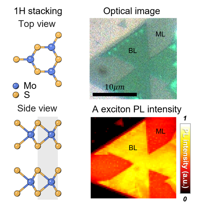
Left: Top and side views of the atomic structure models of 1H-stacked bilayer MoS₂. Upper right: Optical microscopy image of 1H-stacked bilayer (BL) and monolayer (ML) MoS₂. Lower right: Corresponding photoluminescence (PL) peak intensity mapping.
The results revealed that the interlayer spacing of 1H-stacked bilayer MoS₂ is approximately 0.674 nm, larger than the approximately 0.617 nm observed in conventional 3R stacking. This difference indicates weaker interlayer coupling in the 1H configuration. Further DFT calculations and ARPES measurements confirmed that this unique atomic arrangement modifies the electronic band structure and produces a direct bandgap, overcoming the conventional physical limitations of bilayer MoS₂.
Beyond the transformation of its electronic band structure, 1H-stacked bilayer MoS₂ also exhibits remarkable optical advantages. PL measurements showed that its integrated excitonic emission intensity is approximately 1.6 times that of monolayer MoS₂ and approximately 6.8 times that of conventional 2H- and 3R-stacked bilayers. Under resonant excitation, the degree of circular polarization of 1H bilayer MoS₂ reached approximately 21% at room temperature, comparable to the 18% observed in monolayer MoS₂. Under nonresonant excitation, its A-exciton valley polarization was approximately twice that of the monolayer.
This research demonstrates that future 2D semiconductor design need not rely exclusively on changing material composition or thickness. Instead, precise control of atomic stacking provides an additional strategy for tailoring fundamental electronic and optical properties. This approach could potentially be extended to ultrathin light-emitting devices, photodetectors, optical information processing, valleytronics, and quantum functional devices, offering new directions for semiconductor technologies and emerging quantum applications in the post-Moore era.
The achievement also highlights the research support capabilities of NCKU's Core Facility Center in advanced materials characterization and interdisciplinary research. The Center integrates sophisticated materials characterization instruments and semiconductor processing facilities while continuously developing in-house analytical and characterization technologies. It provides professional technical expertise and shared instrumentation to research teams within and beyond the university. In addition, the Center actively develops advanced technologies, including custom-built multiphoton microscopy systems, and conducts research related to 2D materials.
Dr. Lin emphasized that this achievement was made possible through the sustained efforts and close collaboration of researchers across multiple institutions. He expressed his appreciation for financial support from research projects funded by the National Science and Technology Council and the Taiwan Consortium of Emergent Crystalline Materials. He also acknowledged the support provided by NCKU and its Core Facility Center in research resources, professional expertise, and advanced instrumentation. These contributions enabled the interdisciplinary research concept to be progressively realized and ultimately published in a leading international scientific journal, demonstrating Taiwan's research capabilities in 2D semiconductor materials.
